"Life moves pretty fast, if you don't stop and look around once in a while, you could miss it."
- Ferris Bueller
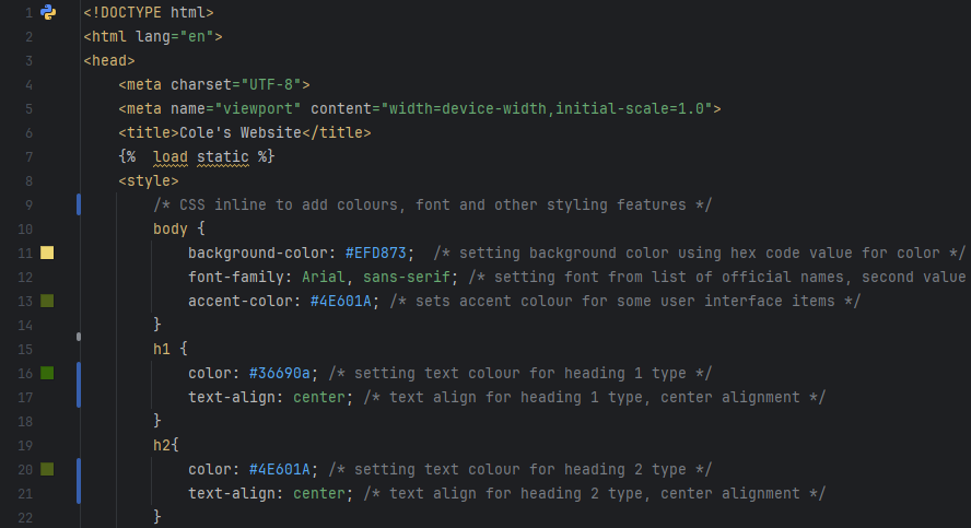
- This personal website is an ongoing project to engage audiences as well as track both my contributions and growth throughout my career.
- I manually coded the site using python based development framework Django to allow for easy addition of more complex features in the future.
- The main static webpage of course is majority CSS/HTML which has given me a great deal of appreciation for what goes into even the simplest examples of front-end web development.
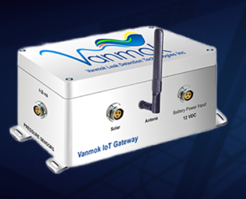
- Independently designed schematics and layouts of a main IO board + LoRa, LTE-M, and LTE-4G module card designs.
- This also included the identification and remedying of several issues from the previous version of gateway like voltage droop affecting RF chips due to insufficient local decoupling, thin power traces, and minimum used operating voltage for of RF chips, non-ideal coplanar waveguides for RF signal paths, lack of dedicated ground plane, and other minor improvements.
- This device is a companion for a true PLC feeding it relay controlled outputs for connecting with SCADA. The re-design consisted of several bug improvements I identified like in the reverse-polarity protection, various components exceeded their maximums like the pmos in the reverse-polarity scheme, reversal of relay logic - HIGH logic now the default state for NC contacts, this solved issues where client would receive false alarm during brief power loss, and also added measures to further prevent undefined states with newly added pull-downs.
- Designed a new version of signal tester (LTE-M and 4G) that will be marketable to clients.
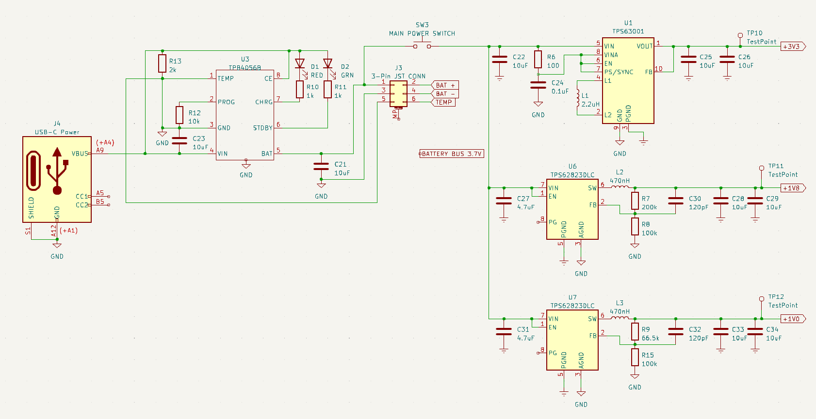
- Identified issues with and refined proprietary solar charge controller, critically, reducing the footprint and complexity of the board - streamlined design by converting design to fully 3.3V logic/peripherals.
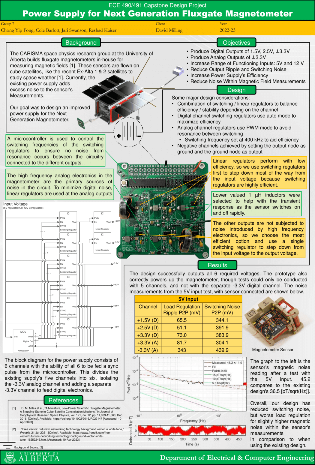
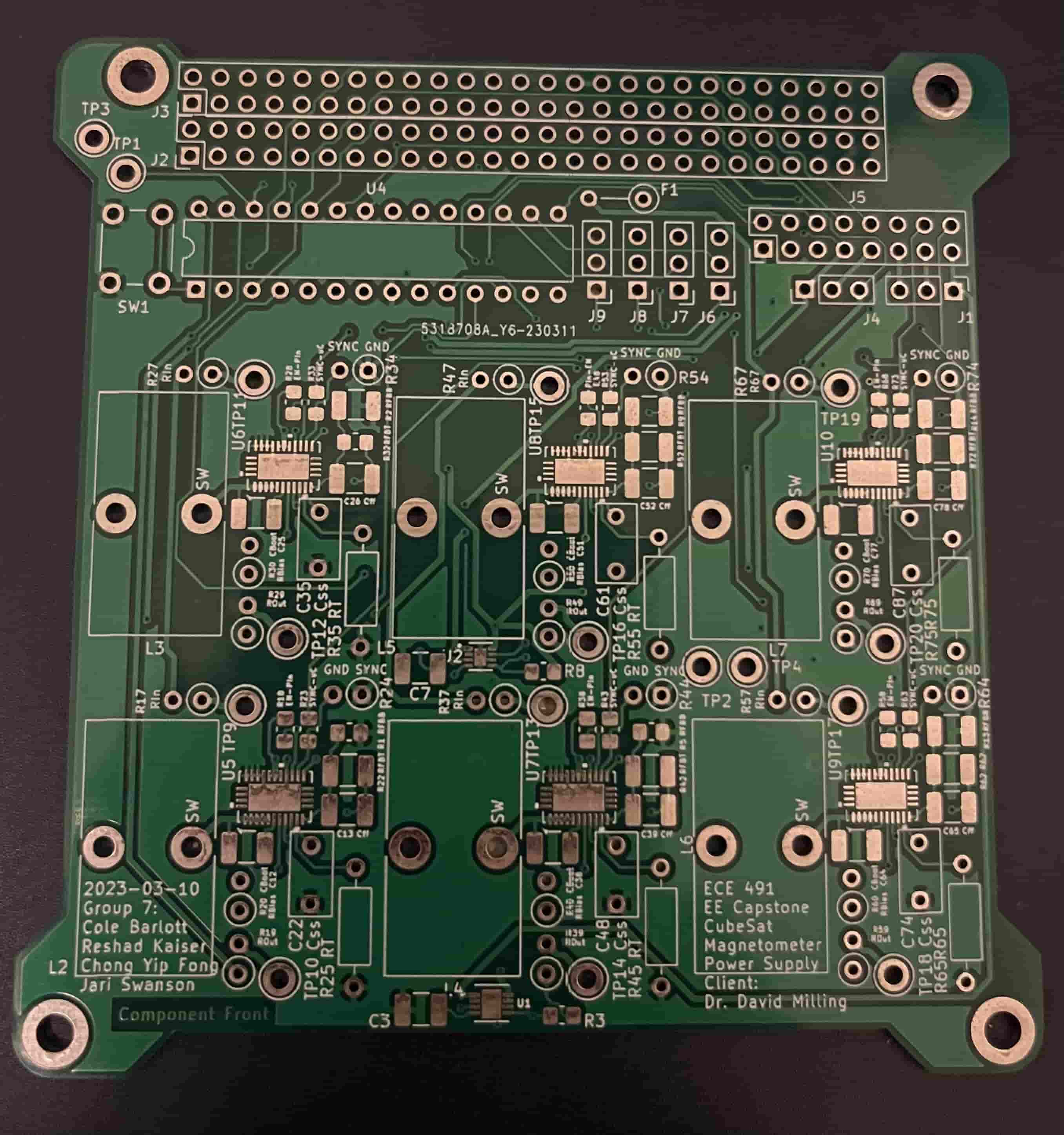

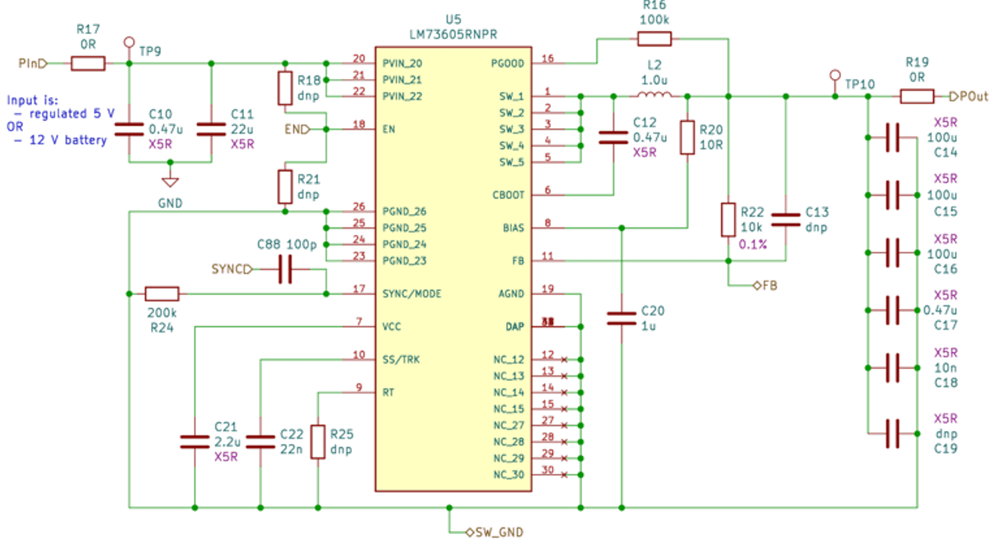
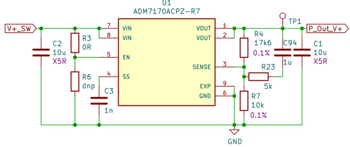
-Led redesign of magnetometer’s 6 channel PC104 DC-DC power supply for UofA space physics research lab.
- Personally solved issues of start-up through soft-start capacitors, of switching regulators not entering PWM mode
from improperly set up sync-pulse and when using inverting buck-boost topology for negative outputs by adding
a level-shift circuit, inability of group members to set up functioning IBB converters and negative linear regulators,
and solely finalized the key sub-circuit inductor/capacitor/switching frequency values of final design.
- Worked first-hand on drafting Requirements/Specifications document from client’s input, parts list and BOM,
bi-monthly progress reports, prototyping stage on breadboard/PCB, MCU programming, and final report.
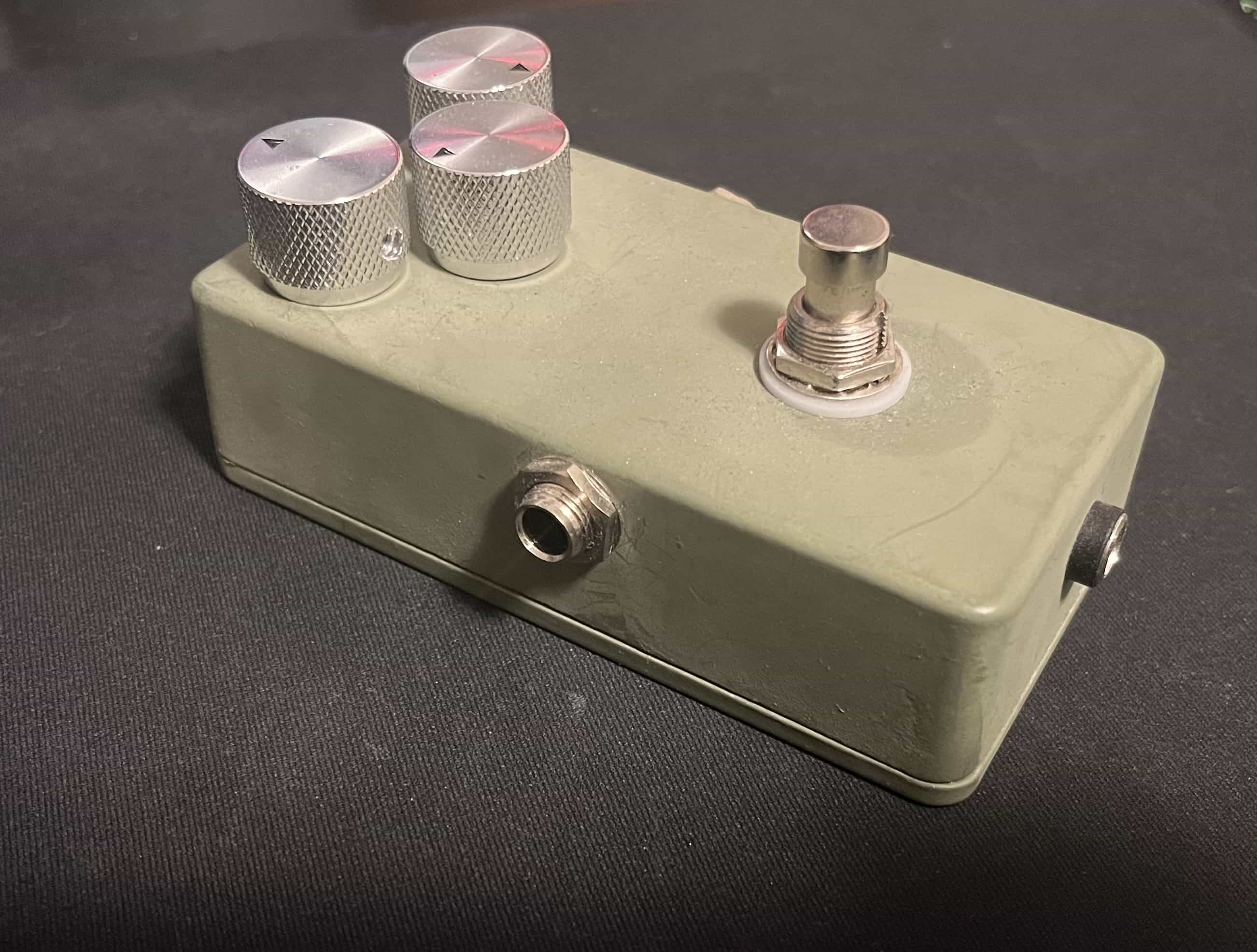
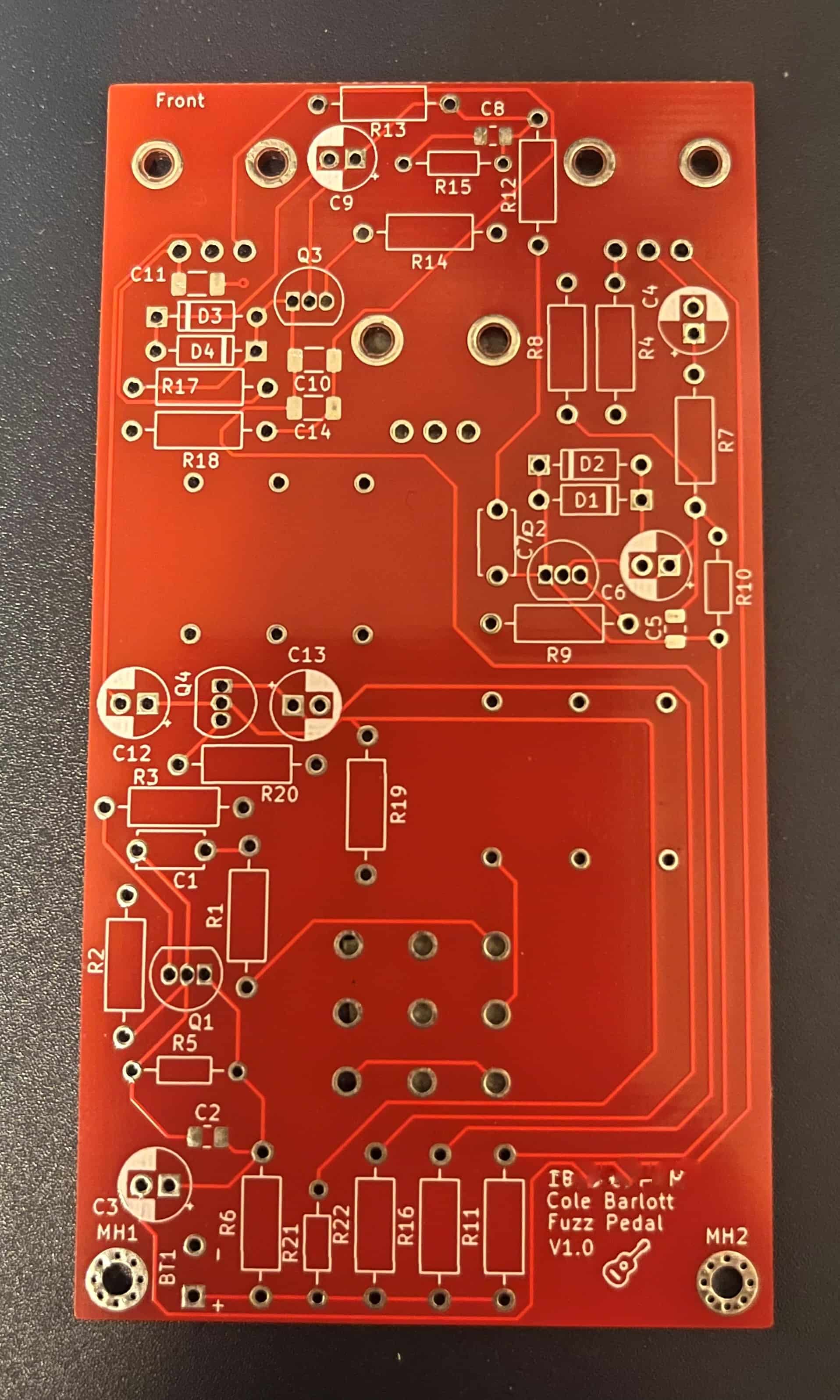
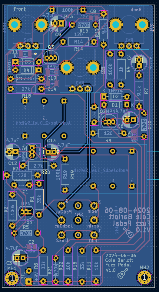
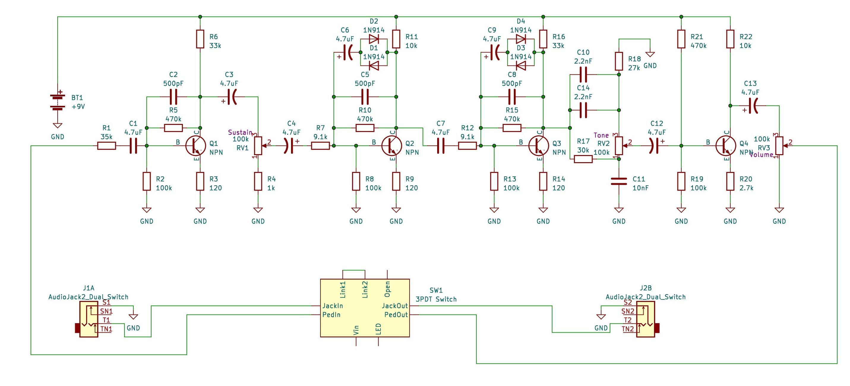
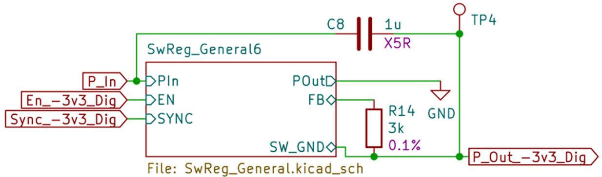
- Designed and built a custom fuzz guitar pedal which takes input sine waves from electric guitar
pickup and outputs square-esque waves with volume, tone, and sustain control.
- This included parts selection, fine-tuning of schematic for preferred sound through breadboard prototyping and
LTspice simulations, custom PCB design, and assembly.
- Solved issues of transistors not turning on by increasing base voltage to ~0.7V by decreasing C-B resistance; and
lack of gain in volume transistor by increasing the ratio of C:E resistors

- Independently led team collecting field data in live plant for assessment of EHT (Electric Heat Tracing)
system, the creation of 40+ new drawings,
quality checked all drawings and prepared results/report for
client myself and assisted in client meetings.
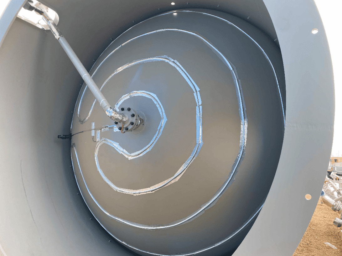
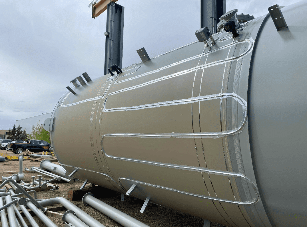
-Shown is the installed electric heat trace for one of client's vessels, designed myself.
- 240V Input, 3 Circuits, RTD control, Thermon HTSX 15-2 Cable for this specific vessel.
-Independently led entire design of EHT circuits and deliverables for 11 Vessels total.
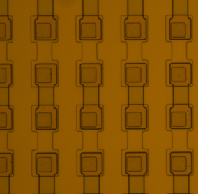
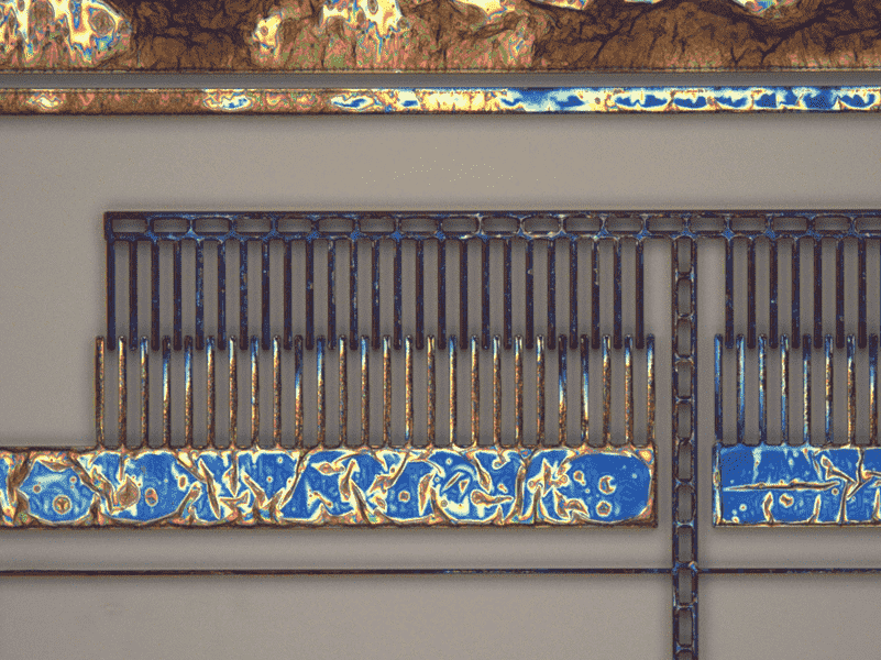
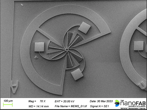
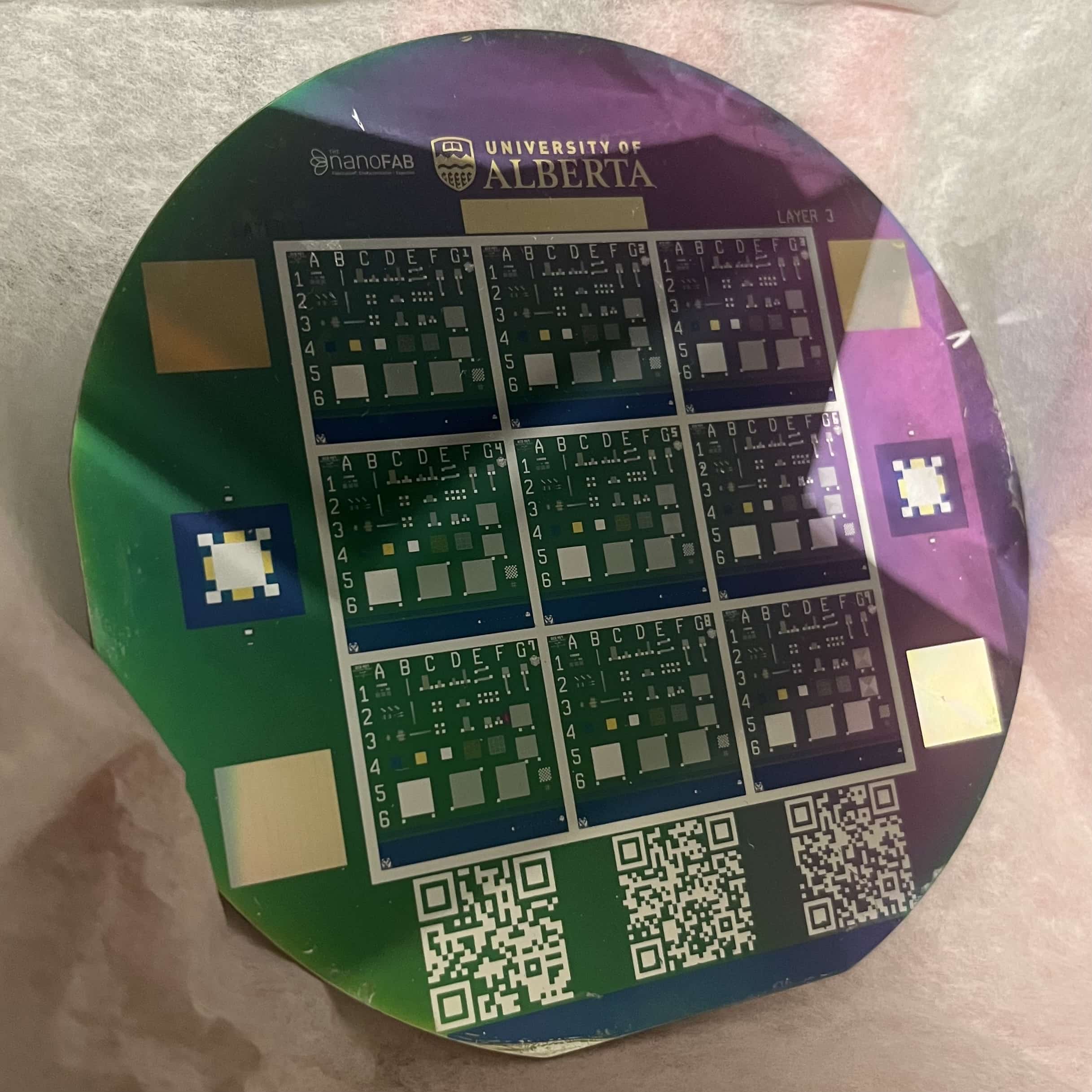
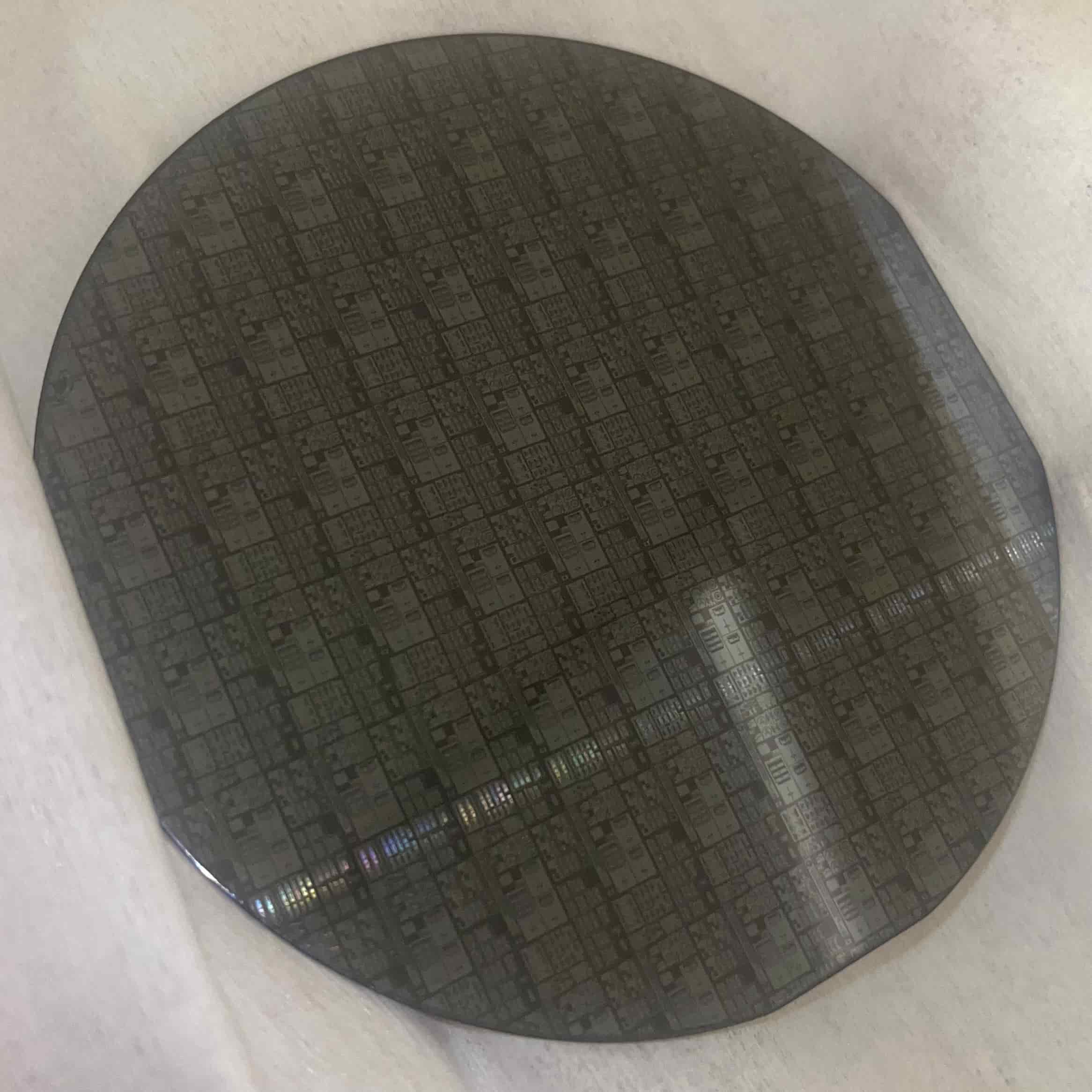
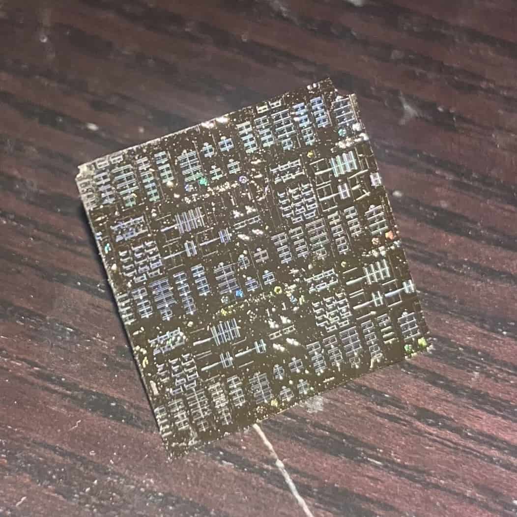
-2 main microfabrication projects completed in the UofA nanoFAB clean room.
-1st where a P-type silicon wafer was processed to create working multi-layer structures such as Via Chains, Greek/Kelvin Crosses, and Serpentine Resistors.
-2nd Wafer was a P-type SOI wafer processed to achieve functioning MEMS devices such as Comb drives, spiral drives, beams, and micro-grippers.
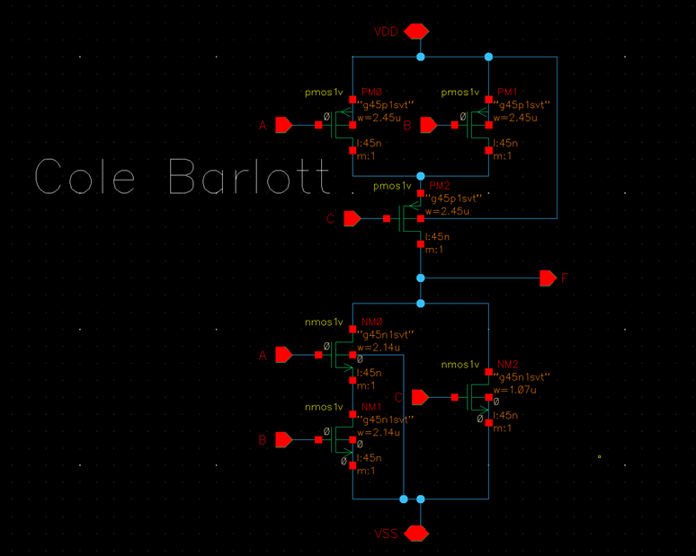
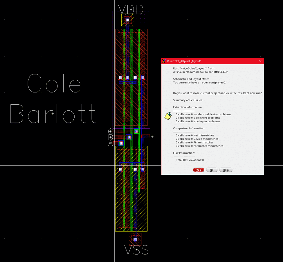
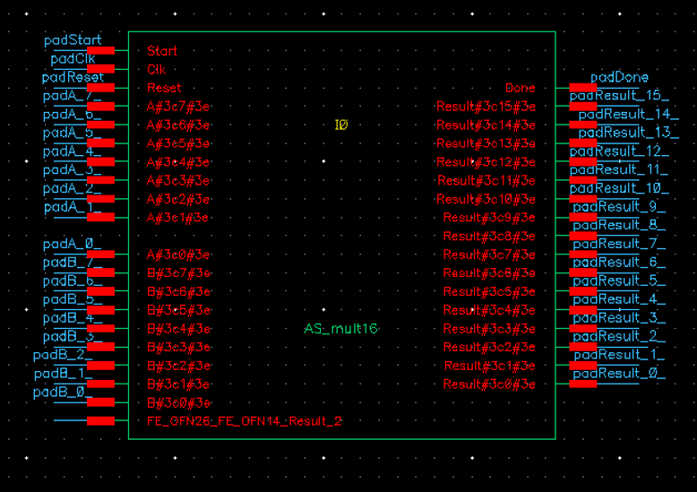
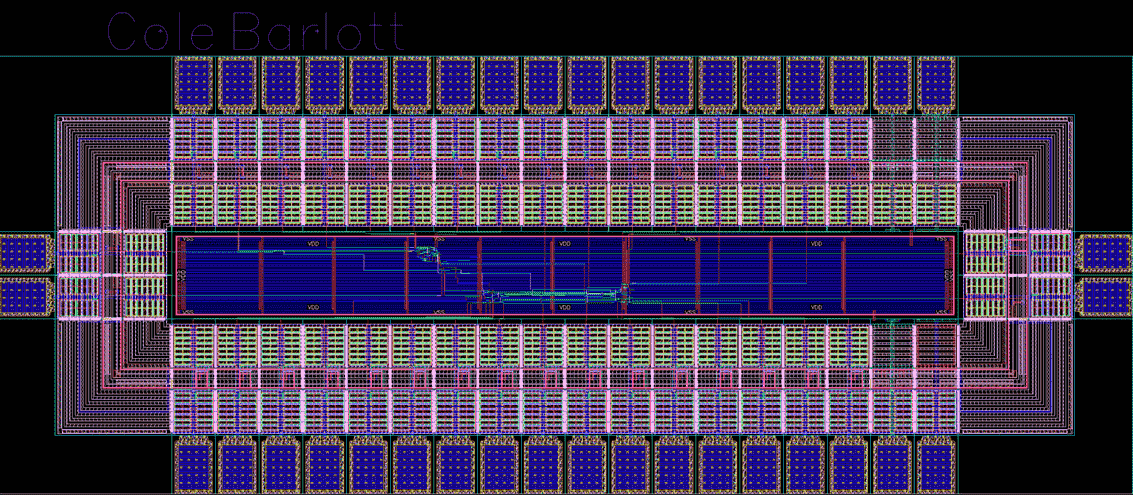
-Integrated circuit design lab consisted of several projects ranging from fully custom design and layout (NOT(AB+C) Chip) and largely automated design/layout using tools with manual connections (8x8 Multiplier) completed using Cadence Virtuoso. DRC and LVS verified.
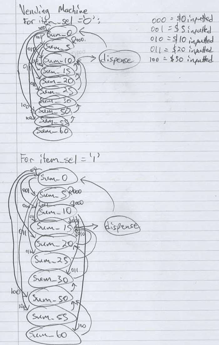
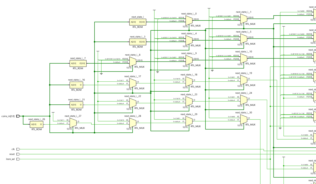
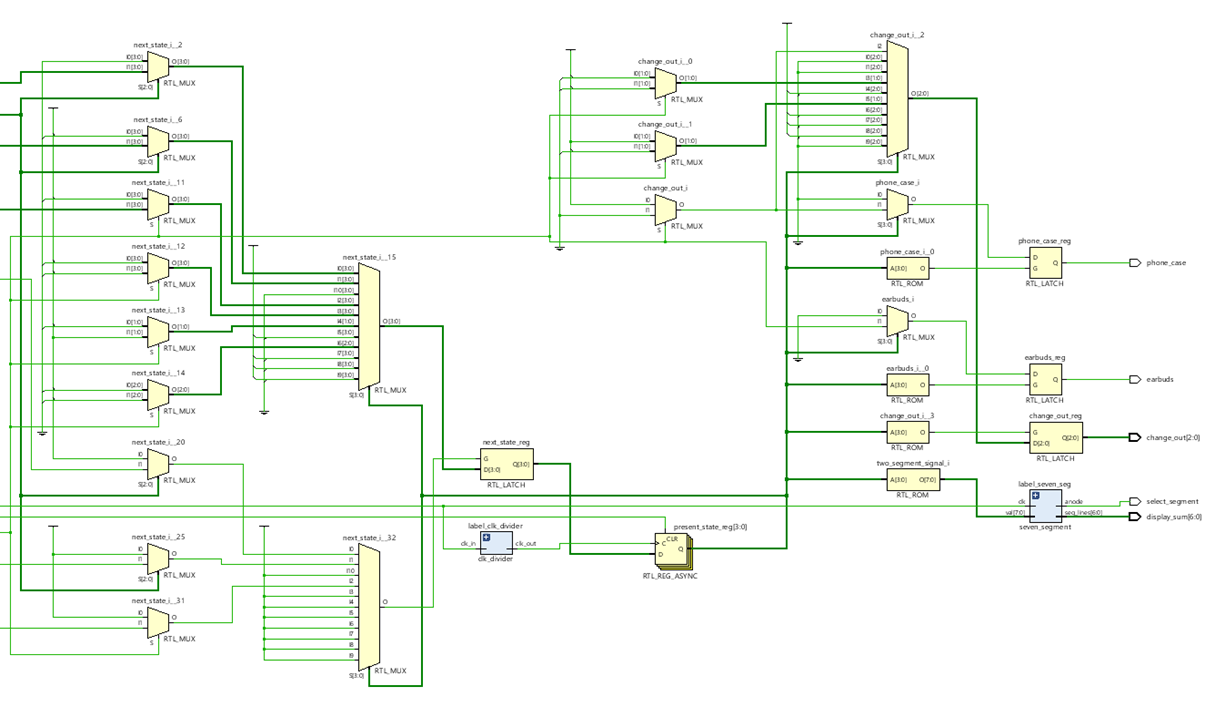
-10 State design consisted of state diagram creation, button/switch/7-segment display mapping in constraint file, VHDL coding, simulation and verification in Vivado, and synthesis of final design onto Xilinx FPGA.